Intel 7nm is equivalent to TSMC's 5nm? ASML reveals the answer
2021-04-10
ASML has become the world’s largest supplier of lithography equipment and the source pillar of the semiconductor industry. Whether it is Apple’s M1 chip or Qualcomm’s Snapdragon 888 chip, they were all born under ASML’s lithography machine. In the lithography machine market, ASML has occupied 62% of the global market share, not to mention EUV is the only one.
ASML's main customers are companies such as TSMC, Samsung, Intel and SMIC. Although the order for the lithography machine is not a problem, the supply is not a day or two. It can take up to two years from order to delivery. The US$120 million EUV contains more than 100,000 parts and requires about 40 containers for transportation. And most of these parts are from the United States, which is why the United States can restrict the export of lithography machines.
ASML not only produces lithography machines, but also does not lag behind in the research of semiconductor manufacturing. So in their opinion, what are the similarities and differences in the technology of these major semiconductor manufacturers? Anthony Yen, the head of the ASML Technology Development Center and the company’s vice president, said in a recent interview that Intel has fallen behind competitors in the 5nm process, and 7nm has not started mass production, but due to their higher design rules, Intel The 7nm is almost the same as the 5nm of TSMC and Samsung.
With the help of AMD’s advanced manufacturing process from TSMC, both mobile and desktop CPUs have begun to adopt the 7nm process, while Intel’s mobile terminal has finally used 10nm, while the desktop CPU is still using the well-polished 14nm process. For example, the Rocket Lake-S series will be officially released on March 30. Although Intel has carried out multiple iterations of 14nm, in the eyes of users, this time "toothpaste" is too long.
One foot into the full 10nm
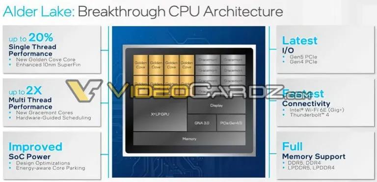
Although Intel has been bumpy on 7nm, fortunately, it is about to enter the stage of full 10nm. Recently, the foreign media VideoCardz announced the leaked information of the Alder Lake-S CPU that may be released in the fourth quarter of this year. Judging from the published news, this CPU does not use the 10nm SuperFin technology on the Tiger Lake mobile processors today, but an enhanced version of the 10nm SuperFin.

As can be seen from the figure above, with the support of new technologies, Intel has once again increased single-threaded performance by 20%, multi-threaded performance by up to twice, and supports the latest PCIe 5.0, Wi-Fi 6E, Thunderbolt 4 and DDR5. The interface of the new CPU will also be changed to LGA1700 for motherboards equipped with Intel's 600 series chipset. But from the industry sources, it is very likely that only high-end Z690 motherboards will provide DDR5 memory support, while low-cost Z690 motherboards may still only support DDR4 memory. It is understood that this is due to the uncertainty of the mass production of DDR5 memory, which also gives Intel and motherboard manufacturers greater market flexibility.
VideoCardZ also broke the news that the 13th-generation chip Raptor Lake-S will be officially released in 2022. It is likely that the 10nm SuperFin enhanced version will still be used, and the 7nm SuperFin enhanced version may have to wait until the future Meteor Lake-S processor will be available. .
Density is not lost, naming suffers
So Intel, which has a backward process, must be worse than TSMC and Samsung? Not at all. It is better to say that Intel's manufacturing process is backward than it is to say that it has suffered a naming loss. Since the 1960s, the semiconductor industry has been using physical parameters as a synonym for process technology, that is, transistor gate length. This generation of nouns has gone from the micrometer level in the 1980s to the nanometer level today, but it has gradually begun to deviate from its original meaning and more similar to a commercial term. Now that the most advanced process has reached 5nm, semiconductor manufacturers such as TSMC have begun to study 2nm and 3nm, giving people the illusion that semiconductor technology is about to reach its limit.
According to Anthony Yen's point of view, ASML firmly believes that Moore's Law can be adhered to for at least another 10 years, and will promote the evolution of the semiconductor industry together with 3D integration technology. At the same time, many people are also calling for new ways to measure the development of process node technology, and Intel is the main caller among them.
Intel senior researcher and director of process architecture and integration Mark Bohr called for standardized density indicators to measure the relationship between the process and the Moore's Law curve as early as 2017. The manufacturing process has been changed, but the density of transistors has not changed. Therefore, he advocated using MTr/mm2 (millions of transistors per square millimeter) as the unit of logic transistor density, in addition to giving the density data of SRAM separately.

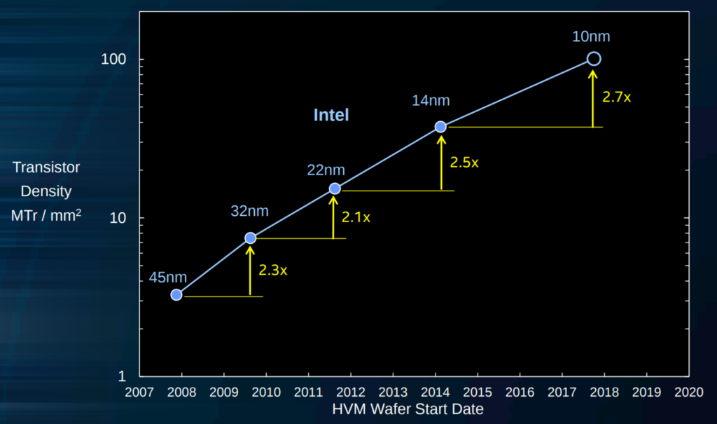
Intel Process Transistor Density Curve / Intel
In comparison with this unit, Intel’s transistor density increase at each process node is very considerable. For example, from 14nm to 10nm, the transistor density has increased by 2.7 times. The 14nm transistor density that Intel has been polishing is 37.5 MTr/mm2, while the transistor density under 10nm has reached 100.8 MTr/mm2.
And TSMC’s first-generation 7nm process N7FF only has a density of 96.5 MTr/mm2. After the introduction of EUV lithography machine, N7FF+ (7nm+) reached a density of 113.9 MTr/mm2, which is currently the main process used by AMD. The density of TSMC's 6nm transition process is around 114.2 MTr/mm2, which is also the process used by MediaTek's Dimensity 1100 mobile phone processor.
TSMC announced in mid-2020 that the logic density of its 5nm process is 1.8 times that of the 7nm (N7) process, so the transistor density is initially estimated to be around 173 MTr/mm2. Compared with Samsung, which also launched 5nm, the transistor density of the latter's 5LPE process is only about 126.53 MTr/mm2. However, Samsung also mentioned before that 5LPE is compatible with 7LPP, most of the design rules are compatible, which means that 5LPE is more like a process renovation after the full introduction of EUV lithography machine.
Brian Krzanich, the former CEO of Intel, mentioned that compared with 10nm, Intel’s 7nm will have a 2.4 times density increase. The last CEO, Bob Swan, mentioned at the end of 19 that Intel will not pursue a 2.4-fold or 2.7-fold increase on 7nm, but will pursue a 2-fold increase like 5nm. It is estimated that the density of Intel's 7nm transistors is about 202 to 250 MTr/mm2.
Now we can see how much Intel’s disadvantages in process naming are. Other semiconductor manufacturers have not been so aggressive in increasing density, and may have changed their numbers to indicate new process nodes after a small increase. However, Intel’s pursuit of process naming is not a small improvement, it can only continuously add a "+" sign to the existing process by improving performance and power consumption. Taking 14+ and 14++ as examples, Intel used a larger gate pitch in exchange for the improvement of high-frequency performance, so that when 10nm was first introduced, its performance was not even as good as 14nm++.
The issue of density index was also mentioned in a paper published by IEEE last year. One of the authors of this paper is also a researcher at TSMC. This article advocates measuring the process from the density of L (logic), M (memory), and C (connection). L is the density of logic transistors, which is similar to Intel’s main density index, M is the density of the main memory (that is, off-chip DRAM), and C is the connection density between the logic unit and the main memory, so some of the current manufacturing technologies It can be expressed in such a way as [38M, 383M, 12K], and it can also make people see the impact of 3D integration technology on density. In this way, these semiconductor companies can still use their favorite names to promote the technology, but this density index can also serve as a clearer comparison between customers and users.
summary
Although Intel's 7nm has been recognized by ASML, semiconductors are a rapidly changing market, and it is not TSMC that has delayed the progress of the manufacturing process. It is important to know that under the current roadmap, Intel’s 7nm process is expected to accelerate mass production from 2022 and will enter full mass production in 2023. By 2023, TSMC has already achieved full mass production of the 3nm process, even if only 1.5 The density increase of 2 times is also enough to surpass Intel.
Fortunately, Intel does not have to worry too much about the gap in competitiveness even if its manufacturing process lags behind. On March 24th, Intel’s new CEO Pat Gelsinger has announced that it will cooperate with TSMC to be responsible for the foundry of customers and data center CPUs in 2023. In this way, in 2023, Intel can not only fully use its own 7nm process to ensure profitability, but also use TSMC's advanced process after 5nm to ensure competitiveness. Take AMD as an example. The CCD of the Zen 2 series CPU is manufactured by TSMC’s 7nm, but the I/O is based on GlobalFoundries’ 12nm/14nm process. This approach will become more common for Chiplet’s small chip design.
For Intel, which was rigid in design and manufacturing in the past, today Intel has not only opened its own foundry business, but also has not shy away from handing over its own products to third-party foundries. In the future, Intel’s hope of getting rid of the "toothpaste factory" name Keep zooming in.