2021-04-10
The South Korean government recently announced that it will increase the local development of non-silicon power semiconductors for use in electric vehicles and other technologies that require high efficiency and durability. The plan will support the local commercialization of more than 5 types of semiconductors in 2025, including not only silicon carbide and gallium nitride, but also gallium oxide (Ga2O3), which is rarely mentioned.
Compared with conventional semiconductors, power semiconductors can withstand greater voltage and current. At present, gallium nitride has been commercially used in radio frequency power applications such as radar and 5G, and fast charging chargers for gallium nitride have been seen everywhere. In the future, inverters and other devices in electric vehicles will also use this new material. Although silicon carbide is also developing rapidly, due to cost issues, the current penetration rate is not as high as the former. So what are the advantages of gallium oxide, which is known as one of the "fourth generation semiconductor materials", what are the market opportunities, and what is the current development situation?
Advantages of wide band gap materials
Gallium oxide is actually not a new type of material. Instead, it has a history of nearly 70 years. In 1952, scientists have discovered five variants of it. But because this material is ignored by most semiconductor researchers and engineers, its development lags behind materials such as gallium nitride and silicon carbide. It is only in recent years that the semiconductor industry has begun to perceive the excellent characteristics of gallium oxide in the application of optoelectronic devices, and Japan is the main research area for this material.

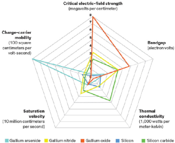
Comparison of characteristics of gallium arsenide, gallium nitride, gallium oxide, silicon, and silicon carbide / IEEE
One big reason why GaN can give devices unprecedented performance is due to its band gap. The wide band gap allows the material to withstand higher electric field strength. The band gap of silicon is as low as 1.1 eV, while the band gap of silicon carbide is 3.3 eV, and the band gap of GaN is only 3.4 eV. Gallium oxide of approximately 5 eV has a great advantage. It can also be seen from the IEEE test data in the above figure that gallium oxide has an absolute advantage in the critical electric field strength and the forbidden band width.
Gallium oxide is divided into five crystalline forms: α, β, γ, δ, and ε. Among them, β-gallium oxide is the most stable, followed by ε and α. At present, most research and development are aimed at band gaps of 4.7 eV and 4.9. The beta-gallium oxide is carried out between eV. In 2012, Japan's NICT developed the first single-crystal β-gallium oxide transistor, and its breakdown voltage has reached more than 250V. It is necessary to know that gallium nitride has passed this milestone after nearly 20 years of development. Moreover, the growth rate of β-gallium oxide is faster than that of silicon carbide and gallium nitride, and the substrate process is relatively simple.
But for suitable semiconductor materials, a wide band gap is not enough. Gallium oxide also has its own limitations. For example, its thermal conductivity is poor, even lower than that of gallium arsenide. Compared with silicon carbide with strong thermal conductivity, the thermal conductivity of gallium oxide is only one tenth of the former. This means that the heat generated in the transistor is difficult to dissipate, which is likely to limit the life of the device. Secondly, gallium oxide is more difficult to manufacture p-type semiconductors. These two points have also become the limiting conditions for the commercial popularization of gallium oxide, and more energy and talents in the industry are needed to solve them.
Limited market participants
One of the players that has made greater progress in the development of gallium oxide is Japan's FLOSFIA, which has been established for ten years and was originally derived from a research project of Kyoto University. FLOSFIA's main business is to make full use of the physical properties of gallium oxide and develop low-loss power devices with self-developed MISTDRY technology. FLOSFIA also received a 1 billion yen investment led by Mitsubishi Heavy Industries in the E round of investment at the end of March this year.

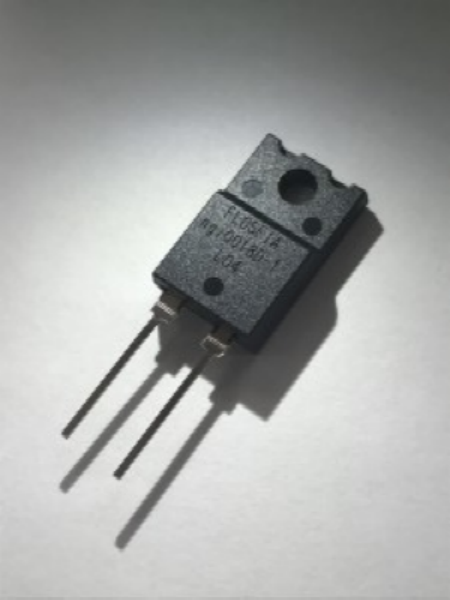
Gallium oxide SBD / FLOSFIA
At present, FLOSFIA has successfully developed an ultra-low on-resistance Schottky diode with an on-resistance as low as 0.1mΩcm2. This is also the world's first gallium oxide power device with a corundum structure. FLOSFIA mentioned that in the gallium oxide power device, they used the sapphire substrate that has been commercialized in the LED. The device not only achieves low loss with ultra-low on-resistance, but also has good high-frequency characteristics, which is very suitable for high-speed switching applications.
FLOSFIA is also developing next-generation gallium oxide automotive power semiconductors with one of its shareholders, Denso. It is worth mentioning that FLOSFIA uses α-gallium nitride. Although β-gallium oxide is more stable, α-gallium nitride has a better band gap, reaching 5.1eV to 5.3eV. In the BFOM index for judging the loss of low-frequency power semiconductors, α-gallium nitride can be nearly 20 times that of silicon carbide.

Market trend of next-generation power devices and related equipment / Fuji Economy
Considering that the technology is not yet fully mature, FLOSFIA's short-term market positioning is still in medium-voltage applications such as household power conditioning, power adapters, UPS, and so on. In the future, it will be advanced to high-frequency communication equipment such as base stations, electric vehicle inverters and industrial motors . Moreover, based on the current power device market analysis data, gallium oxide will only emerge in 2025 and achieve a certain degree of popularity by 2030.
At the International Conference on Electronic Devices in 2019, Ou Xin's group from the Shanghai Institute of Microsystem and Information Technology of the Chinese Academy of Sciences and Hao Yue's group from Xidian University demonstrated wafer β-Ga2O3 single crystal thin film (< 400 nm) and High thermal conductivity Si and 4H-SiC substrates are heterogeneously integrated, and high-performance MOSFET devices are fabricated. With the help of a silicon carbide substrate with a high K value, the device achieves excellent thermal stability, and can still achieve a breakdown voltage of more than 600V at a temperature of 500K.
In addition to research institutions and universities, there is also a domestic high-tech company specializing in gallium oxide materials, gallium technology. Gallium Technology also researches and produces gallium oxide monocrystalline and epitaxial substrates, and has developed gallium oxide-based solar-blind ultraviolet detector discrete devices and array imaging devices from this. Gallium oxide power devices are also discovered by the gallium technology. At present, the gallium family has realized the production of a 1000V withstand voltage Schottky diode model together with its partners, and has realized the production of a 5000V withstand voltage MOSFET model.
summary
Judging from the current development situation, gallium oxide is still in an early stage, and it does not have the strength to compete with gallium nitride and silicon carbide, and it has its own thermal conductivity and structural challenges. But in the long run, the performance potential of gallium oxide is far greater than the current technical obstacles. The two major semiconductor countries in Japan and South Korea have already begun the layout of next-generation semiconductor materials, which shows how big the market for gallium oxide is in the future.
Moreover, gallium nitride does not necessarily act as a competitor in the current semiconductor market. We have also seen the combination of gallium oxide and silicon carbide from the current research progress. Gallium oxide cannot be used in every radio frequency or power scenario. Replace gallium nitride and silicon carbide.